Essentials for Hardware Engineers (Part 1): Current Backflow and Hot-Swap Solutions
2024-03-05 15:57:47 19
Hardware engineers face many more problems and factors to consider when actually designing than what is listed here. Rome was not built in a day, so it takes time and effort.
Thinking about unusual situations
1. Current backflow
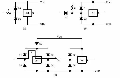
A typical model of an integrated circuit is as follows:

D1 plays an anti-static function in most CMOS integrated circuits. At the same time, it plays an auxiliary role in limiting the input terminal. However, there is no such diode in ABT, LVT, LVC and AHC/AHCT integrated circuits.
D2 is a parasitic diode generated by semiconductor integration (present in all digital integrated circuits). Its auxiliary function is to limit the undershoot signal reflected by the line and provide some discharge protection functions.
D3 is used to protect the CMOS circuit from interference during discharge. This diode is also present in most bipolar devices, but is a parasitic diode. This diode is not available in bipolar devices with open collector and tri-state outputs.
D4 This diode is found in all integrated circuits. It is the collector or drain diode of the device. A Schottky diode is also added to the bipolar device to limit the undershoot signal reflected by the line. Diodes are added to the CMOS circuit to add anti-static functionality.
Causes of current backflow:
When using a CMOS device as an interface chip in the circuit shown below, if Vcc2 is powered off, Vcc1 continues to supply G1, and the high-level output current of G1 will charge the capacitor on Vcc2 through D1 (the charging current will D1 is quickly overloaded and damaged. D1 in CMOS devices can only withstand a current of 20mA) and establishes a voltage on Vcc2, which causes other circuits powered by Vcc2 to work abnormally, especially programmable devices.

solution:

As shown in Figure (a): Adding a current-limiting resistor of several ohms to the signal line can prevent overcurrent from damaging diode D1, but it cannot solve the problem of flooding and establishing a voltage on Vcc;
As shown in Figure (b): Add diode D3 and pull-up resistor R to the signal line. D3 is used to block the perfusion path, and R keeps the input of G1 high when the front-end output is high. This method can solve the problem of flooding that damages diode D1, and can also solve the problem of flooding that establishes a voltage on Vcc. The disadvantage is that the addition of diode D3 reduces the low-level noise margin of G1;
As shown in Figure (c): Add diode D7 to the power supply of G1. The disadvantage is that when the previous stage outputs a high level, G1 obtains the voltage through D1 and outputs a high level to the subsequent stage circuit. At the same time, the power supply voltage of G1 is reduced, so that the high-level output voltage is reduced during normal use.
The most effective solution is to use bipolar devices (such as LS devices, ABT devices) as the interface. Since bipolar devices do not have a protection diode D1, there is no above-mentioned sinking path. It should be noted that no pull-up resistors can be added to the input and output signal lines of the interface at this time (the input of a bipolar device is left floating and treated as high level).
2. Hot-swappable design
Effect of hot plugging on power supply
When the circuit board is powered on or hot-swapped, a large startup current will be drawn from the power supply and cause fluctuations in the power supply voltage. Improper control of this phenomenon will affect the normal use of other circuits in the system and even cause damage to the entire system.
The minimum requirement for a hot-swap circuit is to provide inrush current limiting to prevent damage to the entire system when large capacitive loads are powered. The current limiting feature also helps reduce the size of the power supply and prevents arcing when the connectors make contact. Other hot-swap features include: low equivalent series resistance, circuit breaker, status indication, dual insertion point detection and power-good indication.
At present, our company's products, except for a few processors that take power-on current limiting measures for the power supply, the rest of the circuit boards use PTC to limit load overcurrent, but there is no power-on current limiting measure.
The simplest current-limiting component is the fuse, which can be used alone or in conjunction with other protection components. Since fuses can effectively prevent the impact of overcurrent, they are both necessary in the system (such as UL standards) and are also important when the system encounters The final line of defense in the event of catastrophic failure. The main drawback of standard fuses is that they can only be used once. Another small alternative is a multi-fuse. The physical size of this fuse can expand or shorten based on the heat generated by the current flowing through itself. The working of multi-fuses The voltage range is limited by temperature, but it is self-resetting, which is the biggest advantage over standard fuses.
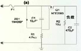
Ordinary hot-swap circuits are composed of capacitors, zener tubes and FETs, as shown in the figure below. The purpose of limiting the surge current is achieved by charging the capacitor C1 connected between the gate and source of Q1. If C1 discharges during power-up, the gate and source of Q1 are equivalent to a short circuit, and Q1 will remain open circuit. When C1 is charging, Vgs increases and Q1 turns on slowly. The size of C1 and the Vgs index of Q1 determine the turn-on time of Q1 and the charging time of the load capacitor C2. Zener ZD1 is used to prevent the gate-to-source voltage from exceeding its maximum rating.

Hot swapping of interface ICs
If the circuit board is not handled properly when powering on or hot-swapping, it will affect the normal use of other circuit boards in the system through the signal lines, and may also cause soft or hard damage to the interface IC. Therefore, the following requirements should be met as much as possible when designing the system and circuit board:
When the circuit board is hot-swapped, the ground terminal must be connected first. This is the basis for the normal operation of the circuit board. In a multi-power supply system, especially a system where negative power supplies are used at the same time, if the ground terminal of the circuit board cannot be connected first during hot plugging, you should try not to use large-capacity capacitors on the negative power supply of the circuit board, because here In this case, the ground potential of the circuit board may deviate to a negative potential, causing the ground voltage of the input and output pins of the interface IC to exceed its tolerance range, causing damage to the interface IC pins.
1. Use ICs without power supply protection diodes on the input or output terminals;
2. Use an IC with power-on three-state function.
The correct circuit board power-up sequence should be:
First, connect the ground of the circuit board;
Next, connect the power supply of the circuit board;
Connect the reset terminal of the circuit board;
Finally connect the signal terminals of the circuit board;
3. Overcurrent protection
Overcurrent protection technology is commonly used in power supply design and can be used as a reference in circuit board design. Due to abnormal operation or fault damage of the device, the circuit board power supply may be over-current. If this is not restricted, it may bring catastrophic consequences to the system.
Connecting a small-resistance PTC element in series at the power inlet of the circuit board can effectively protect the power supply. When the circuit board generates an overcurrent, the current flowing through the PTC increases, causing the temperature of the PTC to increase and its resistance to increase. The further increase in limiting current limits the current entering the circuit board to a smaller range, which can effectively protect the circuit board without affecting the normal operation of other circuit boards. Another advantage of using PTC is repeatability. When the overcurrent condition no longer exists, the temperature of the PTC drops and the resistance returns to normal, which does not affect its normal use.
When selecting a PTC, you need to pay attention to its withstand voltage, non-operating current, static resistance and operating time.
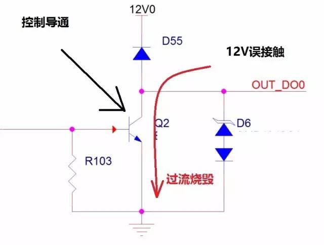
Case: The output of our OC controls the solenoid valve. One end of the solenoid valve is connected to 12V and the other end is connected to OC output. However, during the installation process, it often happens that due to careless construction, OC is directly short-circuited with 12V, causing the triode or MOS tube to directly fail, causing a large number of triodes to be burned out on site.

After optimization, the following circuit can be used to prevent overcurrent and damage to the transistor.


