Master IGBT core technologies: Innovative applications from device structures to emerging topologies
2024-06-24 12:05:28 1157
Igbts (insulated gate bipolar transistors) have long been widely adopted as efficient and reliable technical solutions, even as wide band gap semiconductor materials such as silicon carbide (SiC) and gallium nitride (GaN) are increasingly used today. In fact, IGBT is still the ideal choice for many application scenarios. In this article, INFINITECH will describe the structure and operation of IGBT devices, as well as demonstrate a range of circuit topology designs for different IGBT applications. In addition, we will explore innovative applications of IGBT technology in emerging topologies to show how this versatile and robust technology continues to evolve to meet changing industry needs.
IGBT device structure
In short, an IGBT is a power semiconductor device consisting of a four-layer alternating P-N-P-N structure that works by applying voltage to a metal oxide semiconductor (MOS) gate to achieve control. This basic design is constantly adjusted and optimized, significantly reducing energy loss during switching and making the device itself thinner and lighter. The latest IGBT technology incorporates a channelled gate structure and a field cutoff design to effectively suppress the internal parasitic NPN effect. This method not only reduces the saturation voltage and on-resistance of the device, but also greatly improves the overall power density, thus achieving a major breakthrough in performance.
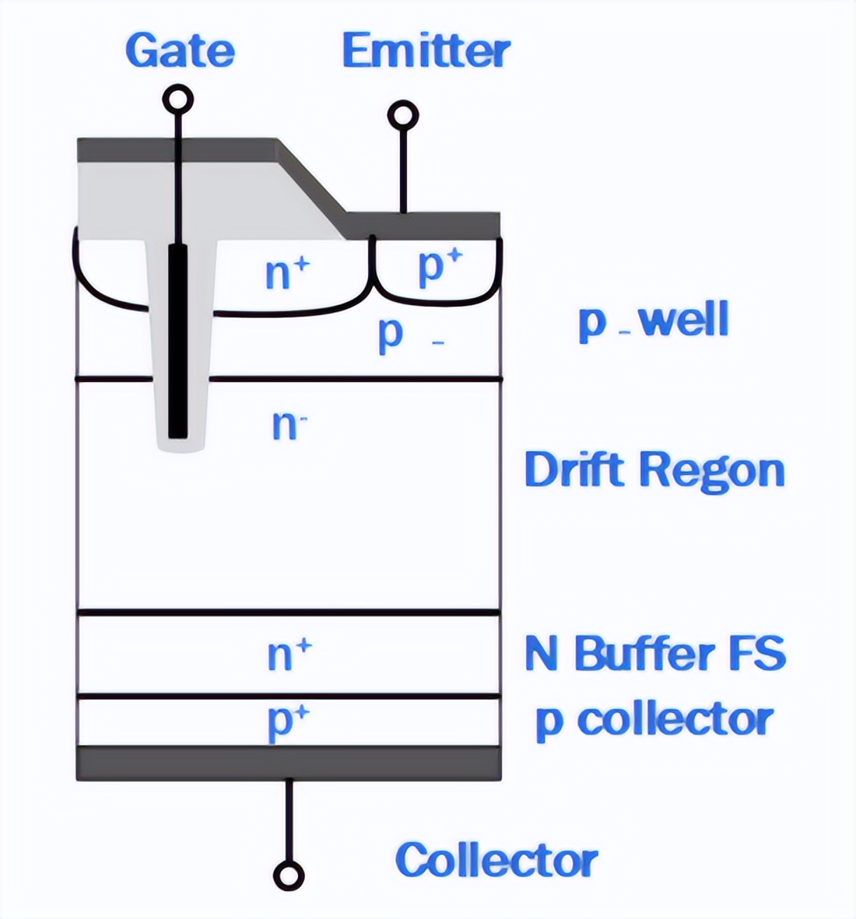 Figure 1: Trench field cut-off IGBT structure
Application and topology
Today, IGBTs are commonly used for application-specific topologies, several of which are listed below by INFINITECH.
Welding machine
Many welding machines today use inverters, rather than traditional welding transformers, because the DC output current can improve the control accuracy of the welding process. There are other advantages to using inverters, such as DC current is safer than AC current, and welding machines with inverters have a higher power density and therefore a lower weight. The power stage (single or three phase) converts the AC input voltage to the inverter's DC bus voltage. The output voltage is usually 30 V, but once the arc is started, the output voltage may be as high as 60 V DC in open load operation almost as low as 0 V (short circuit conditions).

Figure 2: Welding machine block diagram
Topologies commonly used in welding inverters include full bridge, half bridge and two-tube forward excitation, and constant current is the most commonly used control scheme. Duty cycle varies depending on the load level and output voltage. Full-bridge and half-bridge topologies typically have IGBT switching frequencies between 20 and 50 kHz.
 Figure 3: full-bridge, half-bridge, and two-tube forward topologies
Induction cooker
The principle of induction cooker is that when the pot of high permeability material is close to the coil, the current circulation in the pot is driven (or coupled) by the excitation coil. It operates in much the same way as the transformer, where the coil is responsible for the primary side and the bottom of the induction cooker is responsible for the secondary side. Most of the heat generated comes from the eddy current circulating in the bottom of the pan. The energy transfer efficiency of these systems is about 90%, while the energy efficiency of non-inductive electrical devices with smooth tops is only 71%, compared to about 20% energy savings (for the same calorimetric transfer). The inverter directs current into the copper coil, which creates an electromagnetic field that penetrates the bottom of the pan and forms an electric current. The heat generated follows the Joule effect formula, which is the resistance of the pot multiplied by the square of the induced current.
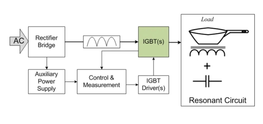 Figure 4: Block diagram of induction cooker
For induction stoves, the more important requirements include:
-
High-frequency switch
-
Power factor close to one
-
Wide load range
Output power control for induction heating applications is usually based on variable frequency schemes. This is a basic method that is applied according to load or line frequency changes. However, this method has a major disadvantage: to control the output power over a wide range, the frequency needs to vary substantially.
The most common topology for induction heating is based on resonant loops. The main advantage of resonant converters is the high switching frequency range without any loss of energy efficiency. Resonant converters use control technologies such as zero current switching (ZCS) or zero voltage switching (ZVS) to reduce power losses. Resonant half-bridge (RHB) converters and quasi-resonant (QR) inverters are popular topologies. The advantages of the RHB structure include a large load operating range and the ability to provide ultra-high power.
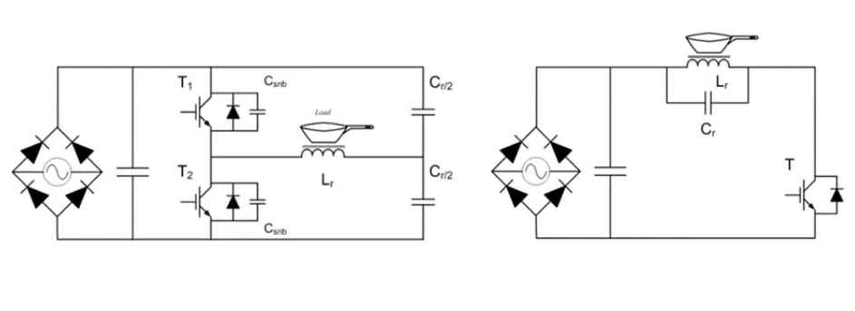 Figure 5: RHB and QR topology
The main advantage of QR converters is their low cost, making them ideal for applications in the low to medium power range (peak power up to 2 kW) and operating frequencies between 20 and 35 kHz.
Motor drive
Half-bridge converters (HB) are one of the most common topologies in motor drive applications, with frequencies ranging from 2kHz to 15kHz. The HB output voltage depends on the switching state and current polarity.
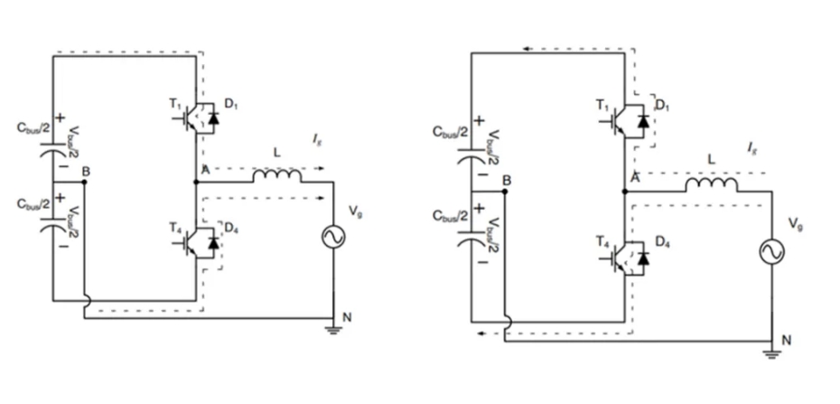 Figure 6: Half-bridge topology showing positive and negative output currents
The current then increases to account for the inductive load. If the load draws a positive current (Ig>;0), it will flow through T1, providing energy to the load (Vg). Conversely, if the load current Ig is negative, the current flows back through D, returning the energy to the DC supply. Similarly, if T4 is on (and T1 is off), a voltage of −Vbus/2 is applied to the load and the current is reduced. If Ig is positive, current flows through D4, returning energy to the bus power supply.
Multi-voltage class topology for IGBT applications
The limitations of fast switching on HB topology include:
-
There are only two output voltage levels
-
Passive and active components are stressed
-
High switching loss
-
Grid drive is more difficult
-
The ripple current increases
-
EMI increase
-
Voltage treatment (cannot be combined with high voltage bus)
-
Devices in series increase the complexity of implementation
-
Thermal equilibrium is difficult to achieve
-
High filtering requirements
To get rid of these limitations, new multi-voltage level topologies are used in applications such as uninterruptible power supplies (UPS) and solar inverters. Common structures include unipolar switching type I and T converters, which are capable of operating at higher bus voltages. As the available output states increase, the voltage between the filter elements decreases accordingly, so the filter loss is also lower and the components are smaller. The switching loss is reduced, while the on-off loss is slightly increased (suitable for higher frequencies of 16kHz-40kHz, which can achieve high energy efficiency of about 98%).
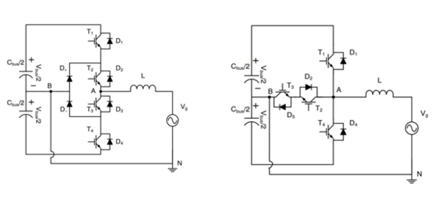 Figure 7: Topology of type I and T converters
The future of IGBT
Although IGBT has been around for many years, the technology is still ideal for many high voltage and current applications. Igbts are increasingly being used not only in traditional designs, but also in new ones, as new devices continue to push Vcesat down to 1V and improve current density and switching losses through new structures. Its future development trend is driven by material science, manufacturing process, design optimization, and application needs. Here are a few key aspects of IGBT's future development:
-
Researchers are exploring the use of new wide-bandgap semiconductor materials, such as silicon carbide (SiC) and gallium nitride (GaN), to replace traditional silicon-based IGBTs. These materials have a higher breakdown electric field, thermal conductivity and operating temperature, which can further reduce device losses, improve efficiency, and allow operation at higher voltages and frequencies.
-
Continue to improve the IGBT structure, such as using a more efficient trench gate structure or optimized buffer layer design, to reduce switching losses and on-off losses, while improving switching speed and reliability.
-
Develop new structures such as FS (Field Stop) and E-TOF (Enhanced Trench Oriented Field) structures to improve performance and reduce manufacturing costs.
-
Integrate more features, such as built-in drive circuits and protection circuits, to simplify system design and improve overall performance.
-
The development of modular technology facilitates mass production and maintenance, while also helping to reduce costs and improve production efficiency.
-
Through improved manufacturing processes, such as epitaxial growth technology and zone-fused silicon single crystal technology, as well as optimized chip design, raw material consumption and production costs are reduced.
-
Integrated intelligent monitoring and diagnostic functions enable IGBTs to self-detect status, predict failures, and achieve a higher level of system management.
-
In the fields of electric vehicles, renewable energy systems, rail transit, industrial motor drives, uninterruptible power supplies (UPS), the application of IGBTs will continue to increase, driving the market growth.
-
Emerging application areas, such as aerospace, medical devices, and high-performance computing, are also likely to become new markets for IGBT technology.
-
Design IGBTs to operate in extreme temperatures, radiation and other harsh environments to meet specific application requirements.
-
The pursuit of higher switching frequencies, lower switching and on-off losses, as well as higher thermal stability and reliability to meet the needs of efficient power conversion systems.
The future of IGBT will be in the direction of higher performance, lower loss, lower cost and wider application, while with the progress of materials science and technological innovation, IGBT will continue to play a central role in the field of power electronics. To get the most out of using IGBTs, a key factor is to first understand the application requirements and then select the right circuit topology to implement.


