Full decoding of the chip manufacturing process: Intel spends $20 billion to reshape the global semiconductor landscape
2024-07-19 14:27:30 907
Some transistors are more than 50 billion in size, and these transistors are 10,000 times smaller than the width of a human hair. They are made on the floor of a huge ultra-clean factory building, up to seven stories tall and the length of four football fields.
Microchips are in many ways the lifeblood of the modern economy. They power computers, smartphones, cars, appliances and many other electronic products. But since the pandemic, the world's demand for them has surged, which has also disrupted supply chains, leading to global shortages.
That, in turn, has stoked inflation and raised alarms in the United States that the country is becoming too dependent on chips made overseas. The United States accounts for only about 12 percent of global semiconductor manufacturing capacity; More than 90 percent of the most advanced chips come from Taiwan.
Silicon Valley giant Intel is trying to regain its longtime lead in chip manufacturing technology by betting $20 billion that it can help ease a chip shortage. The company is building two plants at its chip manufacturing center in Chandler, Arizona, which will take three years to complete. Recently, the company announced plans for a potentially larger expansion, with new plants in New Albany, Ohio, and Magdeburg, Germany.
Why does making millions of these tiny parts mean so much to build and spend? A look at Intel's production facilities in Chandler and Hillsboro, Oregon, provides some answers.
What does the chip do?
Chips, or integrated circuits, began to replace the bulky individual transistors in the late 1950s. Many of these tiny parts are produced on a single piece of silicon and connected together to work. The resulting chips store data, amplify radio signals, and perform other operations; Intel is best known for its various microprocessors, which perform most of the computing functions of computers.
Intel has managed to shrink the transistors on its microprocessors to mind-boggling sizes. But rival TSMC can make smaller components, a key reason why Apple chose TSMC to make chips for its latest iphones.
How are chips made

Rows of specialized machines receive containers filled with chips, which are moved in and out of these systems for processing.
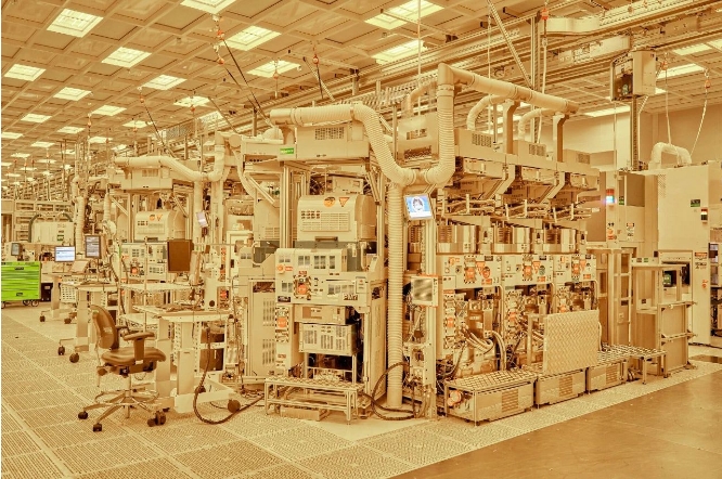 One of the machines is used to etch material from silicon wafers while making chips.
Chip manufacturers pack more and more transistors into each piece of silicon, which is why the technology is increasing every year. It's also why new chip factories cost billions of dollars and few companies can afford them.
In addition to building factories and buying machines, companies have to spend huge sums of money developing complex processing steps to make chips out of flat-sized silicon wafers-which is why these factories are called "fabs."
Giant machines design chips on each wafer, then deposit and etch layers of material to make transistors and connect them. In these systems, up to 25 wafers can be transported at a time in special pods on automated elevated tracks.
It takes thousands of steps and up to two months to process a single wafer. In recent years, TSMC has set the pace for output, operating "gigafabs" with four or more production lines. Dan Hutcheson, vice chairman of market research firm TechInsights, estimates that each plant can process more than 100,000 wafers per month. He estimates that Intel's two planned $10 billion plants in Arizona will have a production capacity of about 40,000 wafers per month.
How to package a chip
 Using new technology, the chips are stacked and then packaged.
 Individual chips are stored on tape and reels before packaging.

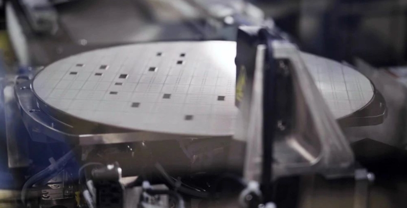 In the packaging process, small "chips" will be bonded directly to the wafer.
After processing, the wafer is cut into individual slices. These are tested and wrapped in plastic packaging attached to a circuit board or part of the system.
This step has become a new battleground because it is harder to make transistors smaller. Now, companies are stacking multiple chips or placing them side by side in a package, connecting them like a single silicon chip.
Packing a small number of chips together is now routine practice, and Intel has developed an advanced product that uses new technology to bundle 47 individual chips together, including some made by Taiwan Semiconductor Manufacturing Company (TSMC) and others, as well as chips made in Intel factories.
What makes a chip factory different
 Intel employees wait for moving tool parts in the Intel Campus cleanroom in Hillsboro, Oregon.
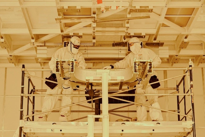 Workers install an automated material handling system in a clean room.
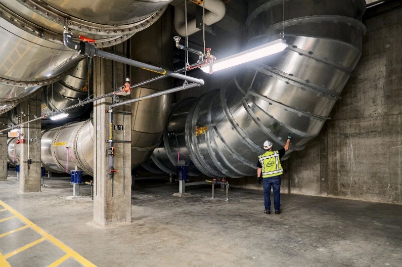 Large pipes drain gas from processing machines at Intel's Hillsboro campus.
Intel chips typically sell for hundreds to thousands of dollars. Intel, for example, released its fastest desktop microprocessor in March, with a starting price of $739. An invisible piece of dust can destroy a person. As a result, fabs must be cleaner than hospital operating rooms, requiring complex systems to filter the air and regulate temperature and humidity.
Fabs must also be protected from any vibrations that can cause expensive equipment to fail. Therefore, the perfect clean room is built on a huge concrete slab, mounted on a special shock absorber.
Equally important is the ability to move large amounts of liquids and gases. Intel's top-of-the-line factory is about 70 feet (21 meters) tall and has huge fans that help circulate air to clean rooms directly below. Below the clean room are thousands of pumps, transformers, power cabinets, utility lines and chiller connected to production equipment.
The need for water in chip manufacturing
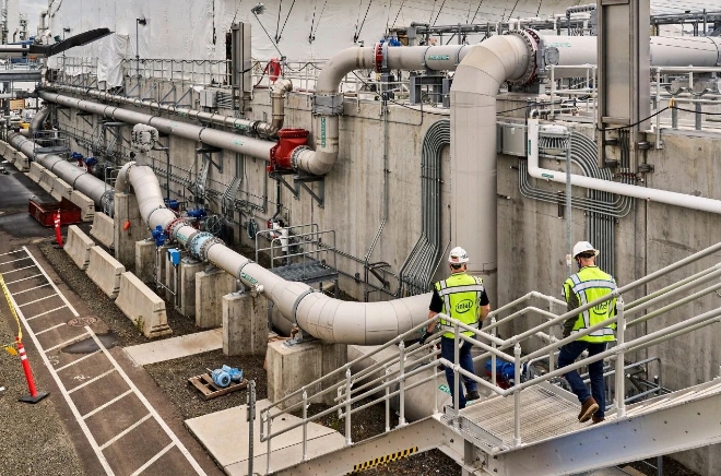 The water treatment plant in Hillsborough. Chip manufacturing requires millions of gallons of water a day.
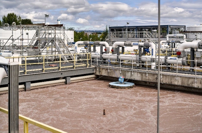 Intel wants to work with environmental groups and others to increase Arizona's water supply by 2030.
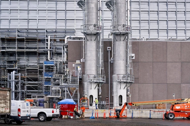 A tower at Intel's Hillsboro plant removes gas from water.
Fabs are a water-intensive business. This is because water is needed to clean wafers at many stages of the production process.
Intel's two sites in Chandler together draw about 11 million gallons (42 million liters) of water a day from local utilities. Intel's future expansion will require more money, which appears to be a challenge for a drought-plagued state like Arizona, which has cut water allocations to farmers. But agriculture actually uses a lot more water than a chip factory.
Intel said its Chandler site, which relies on supplies from three rivers and one well, recycles about 82 percent of its fresh water through filtration systems, sedimentation tanks and other equipment. The water is returned to the city, which operates Intel-funded treatment facilities, and redistributed for irrigation and other non-potable water uses.
Intel hopes to boost water supply in Arizona and other states by 2030 by partnering with environmental groups and others on projects to conserve and restore water in local communities.
Fab construction process

Hillsborough workers carry construction materials.
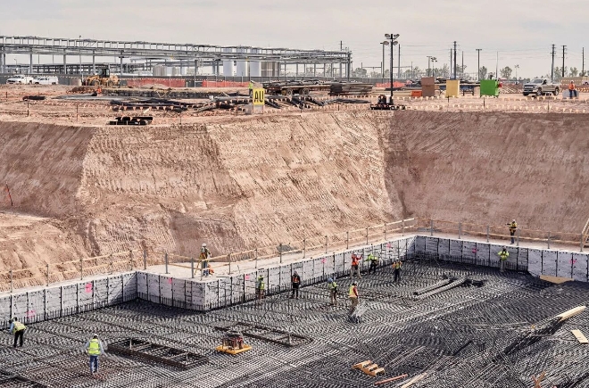 One of Intel's future factories in Chandler. To build its facility, Intel will need about 5,000 skilled construction workers for three years.
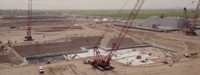 Digging the foundations of Chandler's two new plants is expected to remove 890,000 cubic yards of dirt
 The dirt Chandler dug up will move away at the rate of one dump truck per minute.
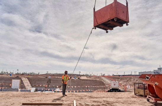 Cranes move construction materials at the Chandler site. Among other things, these cranes will lift 55 tons of chillers for the new fab.
To build the factory of the future, Intel will need about 5,000 skilled construction workers within three years.
They have a lot of work to do. Digging the foundation is expected to remove 890,000 cubic yards of dirt, which is moving at the rate of one dump truck per minute, said Dan Doron, Intel's head of construction.
The company expects to pour more than 445,000 cubic yards of concrete and use 100,000 tons of rebar as the foundation, which is more rebar than was used to build the world's tallest building, the Burj Khalifa in Dubai.
Some construction cranes are so large that it takes more than 100 trucks to put the parts together, Doron said. These cranes will lift 55 tons of coolers for the new fab.
Patrick Gelsinger, who became Intel's chief executive a year ago, is lobbying Congress to fund chip plant construction and provide tax credits for equipment investment. To manage Intel's spending risk, he plans to focus on building fab "casings" that can be equipped with the appropriate equipment to respond to market changes.
To address the chip shortage, Gelsinger will have to go through with his plan to produce chips designed by other companies. But a company can only do so much; Products like phones and cars require parts from many suppliers, as well as old chips. In the field of semiconductors, no country is immune. While boosting domestic manufacturing can mitigate supply risk to some extent, the chip industry will continue to rely on a complex global network of companies to provide raw materials, production equipment, design software, talent and manufacturing expertise.


