【 Comprehensive analysis 】12 Switching mode power supply (SMPS) topologies: non-isolated and isolated details
2024-06-17 11:11:33 825
Switching mode power supplies (SMPS) use power electronic devices (such as MOSFETs, IGBTs, etc.) as switches to switch the connection between the power supply and the load at high frequencies, thereby regulating the output voltage and current. This power supply is generally more efficient than traditional linear power supplies and can provide a smaller volume and higher power density.
The topology of a switching mode power supply refers to the layout and connection of its internal components, mainly including power electronic switches, energy storage components (such as inductors and capacitors), transformers, rectifiers, and feedback control loops. Different topologies are suitable for different applications, based on the desired voltage conversion direction (boost, buck, or both), isolation requirements, input/output voltage range, power level, cost, and size.
Today, INFINITECH wants to share with you the topology of 12 switching mode power supplies, including detailed circuit diagrams, related calculation formulas and their specific applications.
Summary of 12 switching mode power supply topologies
Let's get right to the point. Here, we divide switching mode power supply topologies into two broad categories: non-isolated and isolated. Next, I'll show detailed diagrams of each of these types of structures.

Non-isolated topology summary

Summary of isolated topology
Here is a brief summary of how to choose a switching mode power topology:
 The following describes each switching mode power topology in detail.
1. Buck
Buck
As one of the simplest and most common structures, the BUCK topology is well suited for use as a buck type DC-DC converter. It can not only achieve efficient energy conversion, but also support high power application scenarios. However, one disadvantage of BUCK converters is that their input current can appear intermittent, which can cause high electromagnetic interference (EMI). However, by using filter elements such as chip magnetic beads, common mode chokes and filter chokes, EMI problems can be effectively solved, thus ensuring the stability and reliability of the system.
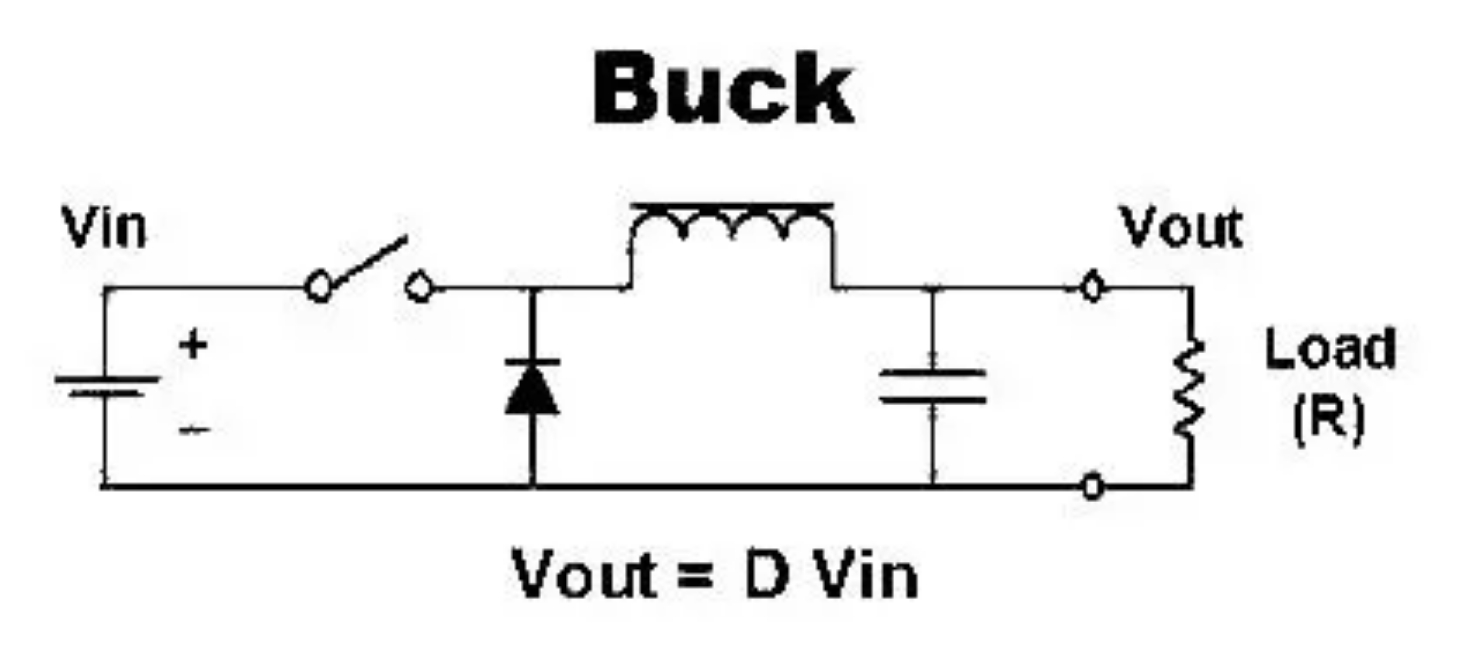 Buck circuit formula
 1) Input and output voltage relationship
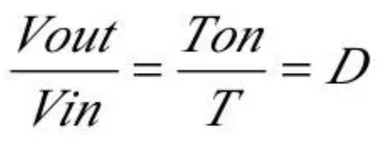 2) The current through the transistor switch

3) Voltage in the transistor switch

4) The current through the diode
 5) Reverse voltage in diode

2. Boost
Boost
Like the BUCK topology, the Boost topology is also non-isolated, but its purpose is to boost voltage. A notable feature of the Boost topology is its ability to absorb current in a continuous and uniform manner when operating in continuous on-mode, a property that makes it ideal for building power factor correction circuits.
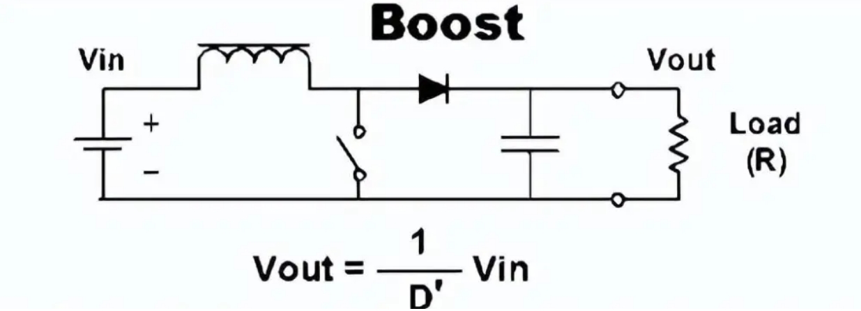 Boost formula
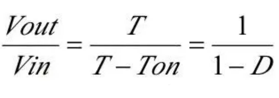
 1) Input and output voltage relationship
2) The current through the transistor switch
 3) Voltage in the transistor switch
 4) The current through the diode
 5) Reverse voltage in diode

3. Buck-Boost
Buck-Boost
The Buck-Boost topology offers both Boost and Buck functions, which makes it particularly useful in battery-powered applications where input voltage can fluctuate over time and Buck-Boost topology can be flexible. However, the output voltage of this topology has the limitation of inverting, which is one of its major disadvantages. In addition, another shortcoming of Buck-Boost topology is that its switches are not directly grounded, which presents certain challenges for the design of the drive circuit. However, it is worth noting that the inductors and EMI components required for Buck-Boost topology can be easily implemented using just one inductor, simplifying the circuit design.
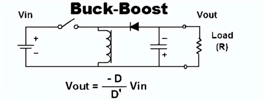 Buck-Boost calculation formula
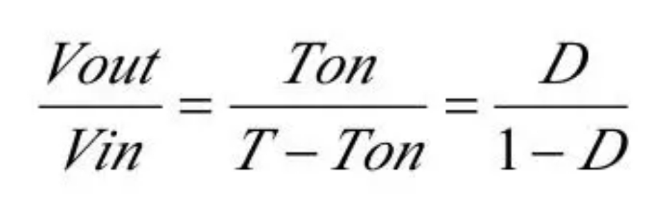
 1) Input and output voltage relationship
 2) The current through the transistor switch

3) Voltage in the transistor switch
 4) The current through the diode

5) Reverse voltage in diode

4. Sepic
Sepic
If you are unhappy with the inverting nature of the output voltage relative to the input voltage in Buck-Boost topology, then a single-ended primary inductor converter (SEPIC) may be an option worth considering. SEPIC is a DC/DC converter topology that provides a stable positive output voltage as the input voltage varies from above the output voltage to below the output voltage. Unlike Buck-Boost topology, SEPIC does not produce reverse voltage, making it a step-down/boost converter topology with no inverting output voltage. Although SEPIC converters require an additional inductor and a straight capacitor to maintain normal operation, their continuous input current consumption helps reduce electromagnetic interference (EMI), which is a significant advantage. However, one disadvantage of SEPIC topology is that it requires more physical space, which means that more layout and size requirements need to be taken into account when designing.
 Sepic calculation formula

1) Input and output voltage relationship
 2) The current through the transistor switch
 3) Voltage in the transistor switch

4) The current through the diode
 5) Reverse voltage in diode

5, the uk
In addition to the two inductors, both SEPIC and the uk topology use capacitors to store energy. The two inductors can be separate inductors or a single component in the form of coupled inductors.
Both topologies are similar to buck-boost topologies in that both can boost or buck the input voltage, making them ideal for battery applications.
SEPIC has an additional advantage over the ZUK and buck-boost converters because its output is non-inverting. One advantage of SEPIC/ SEPUK topology is that capacitors can provide some limited isolation. Coupled inductors can be used in SEPIC and uk topologies, and custom inductors are always available to meet special needs.

6. Flyback
flyback
Flyback is essentially a buck-boost topology, isolated by using a transformer as a storage inductor. The transformer not only provides isolation, but also adjusts the output voltage by changing the turn ratio.
Because a transformer is used, multiple outputs can be made.
Flyback is the simplest and most common topology for low-power applications and is well suited for high output voltages, but peak currents are very high and less well suited for output currents above 10A.
One advantage of flyback over other isolated topologies is that many of them require separate storage inductors. Since flyback transformers are actually storage inductors, there is no need for a separate inductor.
 Flyback calculation formula

1) Input and output voltage relationship

2) The current through the transistor switch
 3) Voltage in the transistor switch
 4) The current through the diode
 5) Reverse voltage in diode

7. Forward type
Forward type
The forward converter is actually a transformer-isolated buck converter. Forward converters are best suited for low-power applications.
Although the efficiency is comparable to flyback, the disadvantage is that the output has an extra inductance, which is not suitable for high voltage output. When high output currents are required, forward converters and flyback converters are more advantageous.
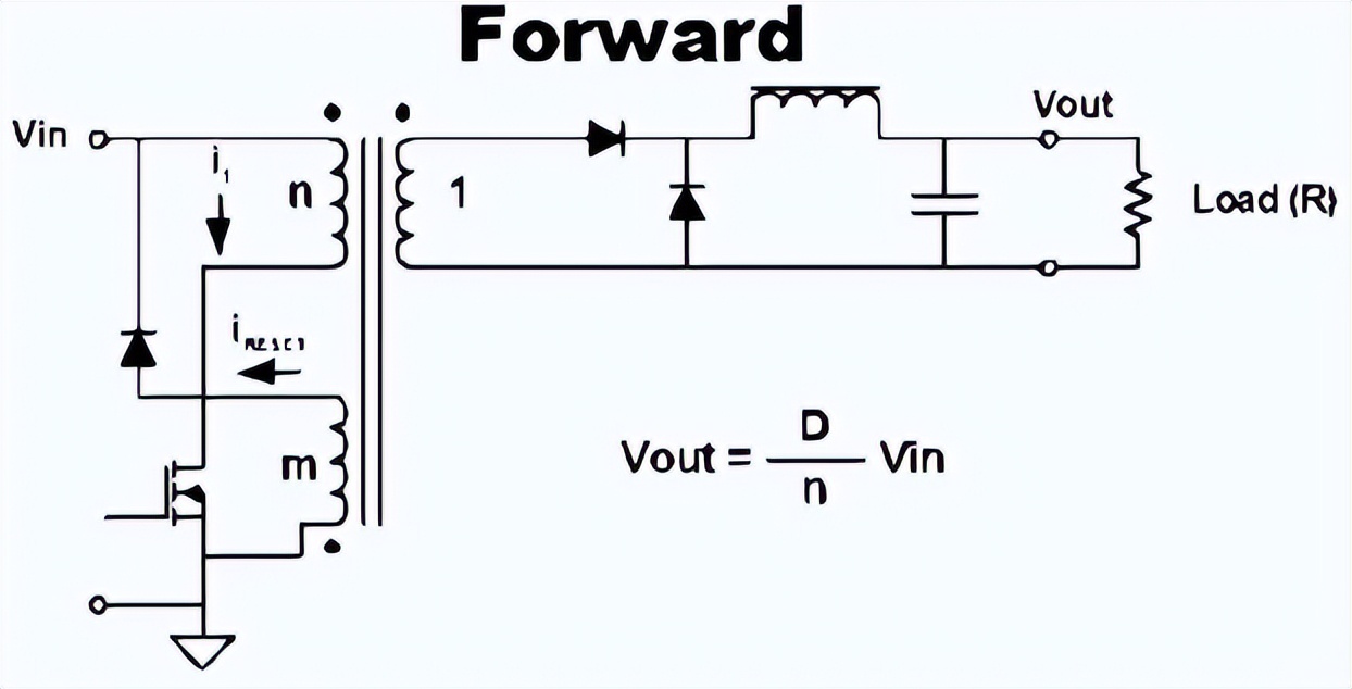
Forward calculation formula

1) Input and output voltage relationship
 2) The current through the transistor switch
 3) Voltage in the transistor switch
 4) The current through the diode
 5) Reverse voltage in diode

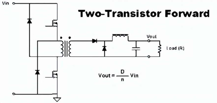
8, dual transistor forward type
Dual transistor forward type
The two-transistor topology is a very reliable design that does not stress the transistor due to voltage spikes.
Because of the isolation between input and output, the dual transistor forward converter belongs to the primary switching converter family. Suitable for output power up to hundreds of watts, both transistors are switched on and off simultaneously by pulse-width modulation control voltage.
 Two-transistor forward formula

1) Input and output voltage relationship
 2) The current through the transistor switch
 3) Voltage in the transistor switch
 4) The current through the diode
 5) Reverse voltage in diode

9. Active clamping forward type
Active clamping forward type
 1) Input and output voltage relationship
 2) The current through the transistor switch
 3) Voltage in the transistor switch
 4) The current through the diode
 5) Reverse voltage in diode

10. Half Bridge
Half bridge
The half-bridge topology, like the push-pull topology, scales well to higher power levels and is based on the forward converter topology. If both switches are turned on at the same time, the topology also has the same straight-through current problem. In order to control this, there needs to be a dead time between the on-time of each switch. This limits the duty cycle to about 45%.
On the plus side, the half-bridge topology switches stress equal to the input voltage, making it more suitable for 250VAC and PFC applications.
On the other hand, the output current is much higher than the push-pull topology, so it is less suitable for high-current outputs.
 Half bridge calculation formula
 1) Input and output voltage relationship
 2) The current through the transistor switch
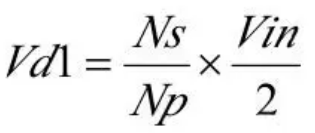
 3) Voltage in the transistor switch
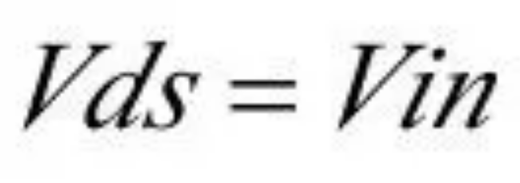 4) The current through the diode
 5) Reverse voltage in diode
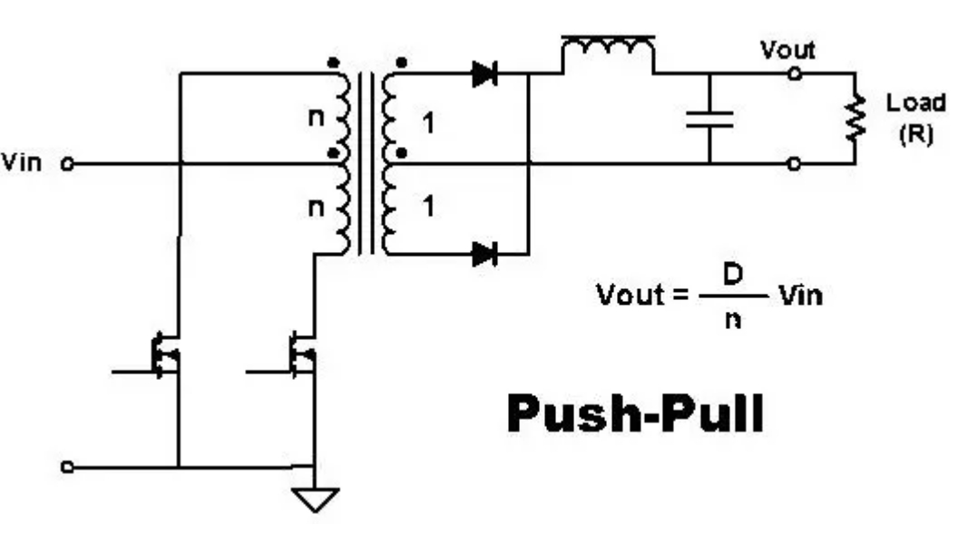
11. Push-Pull
Push-Pull
The push-pull topology is essentially an improved version of the forward converter by using two primary windings to create dual drive windings, which makes more efficient use of the transformer's core resources than flyback converters. However, this method only uses half of the copper wire at a time, which can significantly increase the copper loss of the same size transformer. Push-pull converters typically require smaller filters than forward converters at the same power level. The advantage of push-pull converters over flyback and forward converters is that they can be extended to higher power ranges more easily. However, the switch control of push-pull converters is more complex, and it is necessary to avoid opening two switches at the same time, otherwise equal and opposite magnetic flux will be generated in the transformer, resulting in low impedance and large through-current on the switch, which may damage the switch. In addition, another disadvantage of push-pull topology is that the voltage stress on the switch is very high (up to 2 times the input voltage), which makes it less suitable for 250VAC and power factor correction (PFC) scenarios.
 Push-Pull calculation formula
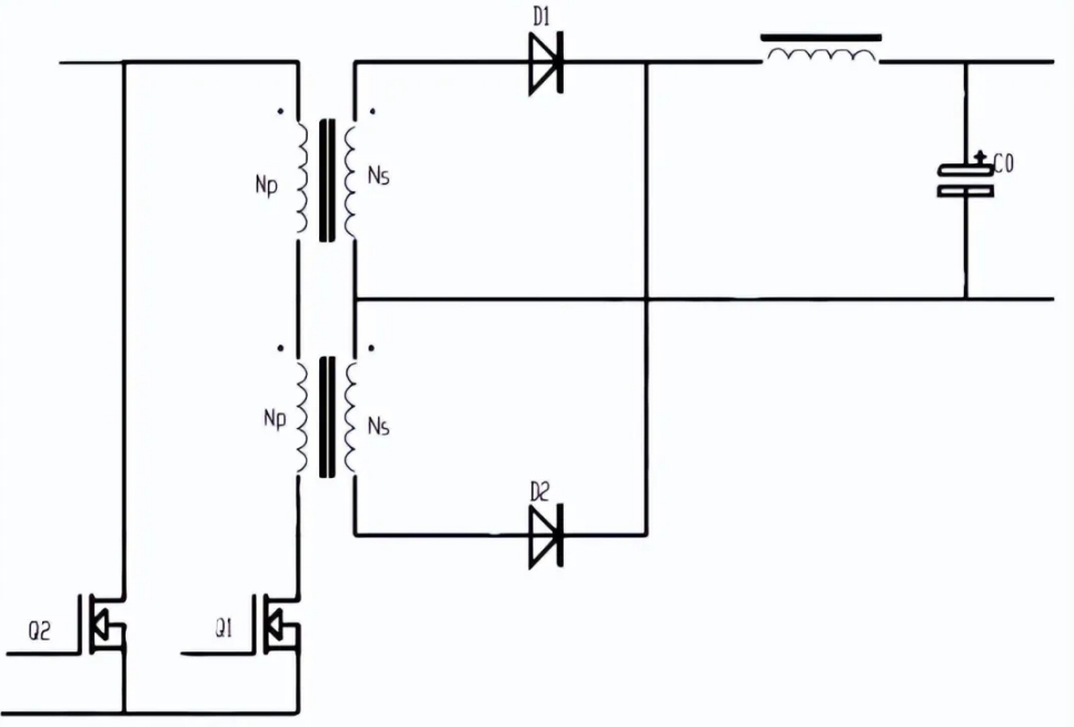
1) Input and output voltage relationship
 2) The current through the transistor switch
 3) Voltage in the transistor switch
 4) The current through the diode
 5) Reverse voltage in diode
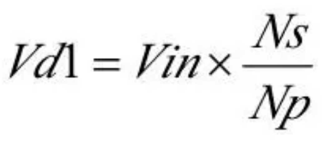
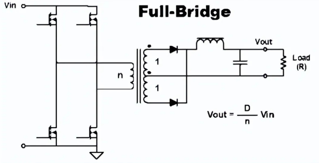
12. Full bridge
The H-bridge consists of four switches that control the current flowing to the load, which is really just a way of controlling the direction of the current with a switch.
For example, to reverse the motor, the power supply must be reversed, which is the role of the H-bridge, the most typical application of the H-bridge circuit is also motor control.
There are a variety of different H-bridge designs, and the actual circuit will depend on the number of transistors, the type of layout, the number of control lines, the voltage of the bridge and many other factors.
One thing that must be very careful when using the H-bridge is not to cause a short circuit. If there's a short circuit, it'll burn the H-bridge.
