Effective Buck Converter EMI Suppression: Case Studies and Practical Tips
2024-05-22 17:16:17 61
Continue with the article "EMC rectification Problem: EMI Source Analysis and Buck circuit Optimization Strategy (Part 1)".
5. Case Study
This chapter will demonstrate the effects of different approaches in the EMI design of Buck converters. The IC used in the demonstration is the RT7297CHZSP, a current mode Buck converter with 800kHz operating frequency and 3A output capability, in the SOP-8 package. The circuit in the test works with 12V input and 3.3V/3A output. The circuit used in the test is shown in the figure below.
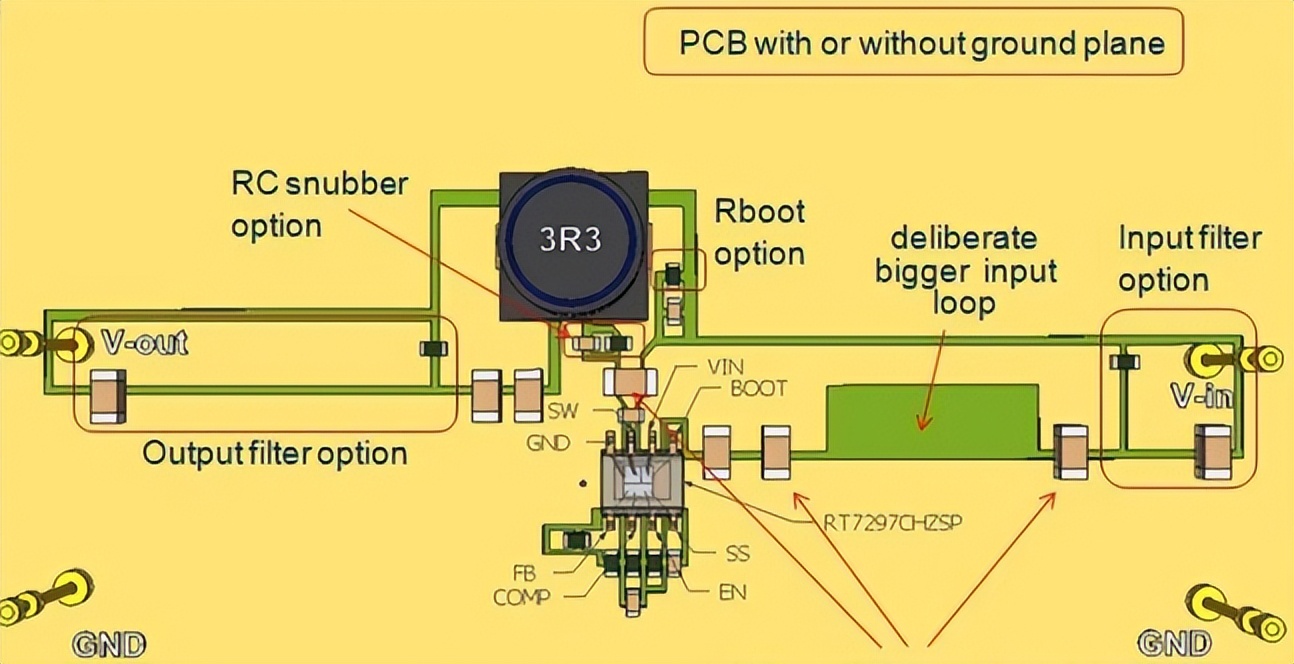
 The board used for the test came in two versions, one with a full floor copper foil layer and one without. Several optional configurations are set up on the board, such as LC input filter, different input capacitor placement positions, optional Rboot, RC buffer circuit and output LC filter. PCB designs with these different options are shown in the figure below.
 The following figure shows the configuration of the test equipment.
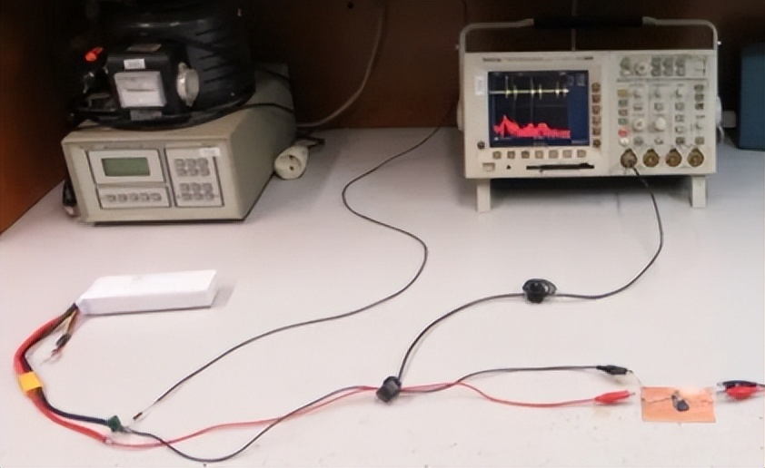 When the test object is placed on the test table, the current loop and wire on its PCB will radiate high-frequency energy to the surrounding environment, and these radiation signals will find their own path back to the test object, and appear on the power supply line in the form of high-frequency common mode current. The high-frequency common-mode current in these supply lines is combined with the current on the plate and can be used as an indication of radiation status.
 The converter's power input comes from three lithium-ion batteries in series, with a voltage of about 12V, which makes them not directly linked to other equipment in the lab. An electrolytic capacitor is attached to the lead of the battery, which eliminates possible resonance problems caused by the battery's inductance.
The converter is loaded with a 1Ω resistor connected in parallel with a 10µF MLCC capacitor, which gives it a 3A load and a very low impedance to high frequency signals.
The input wire is connected to the ground of the test bench by a 100Ω resistor at the ground end of the battery side. This provides a reference point for the entire circuit, and its impedance is much like that of the LISN network in the EMC test.
Placement of input capacitors
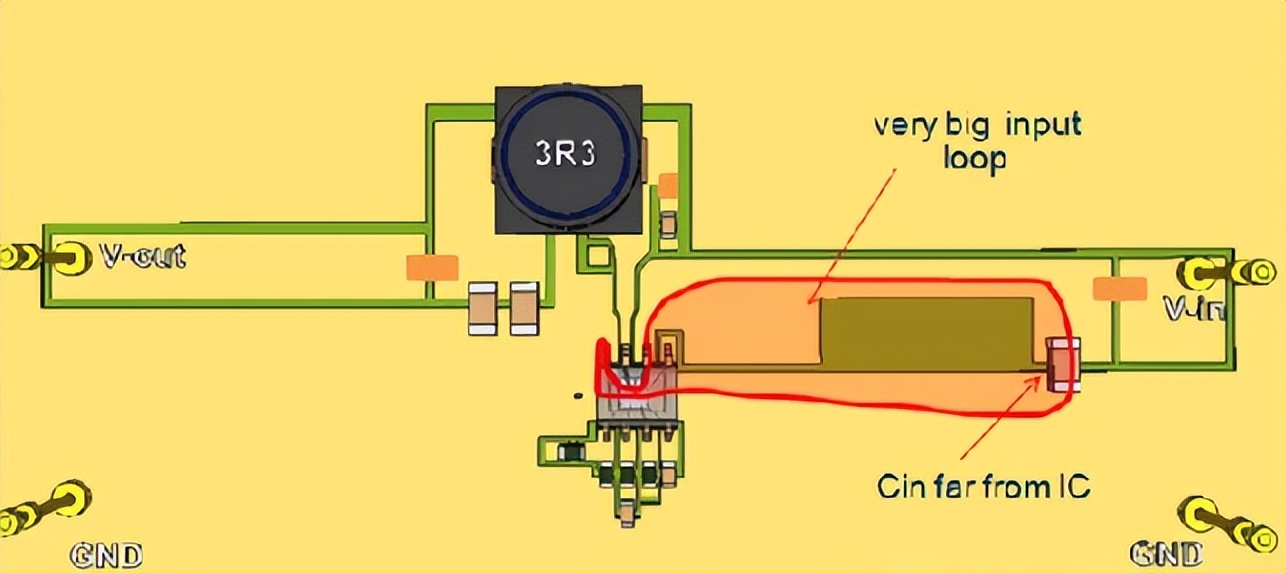
Experiment 1: Place CIN away from IC.
The PCB layout in the figure below presents a poor input capacitor placement method, which will introduce a large parasitic inductance into the switching loop. (There are additional gaps in this layout to increase the area of the loop.)
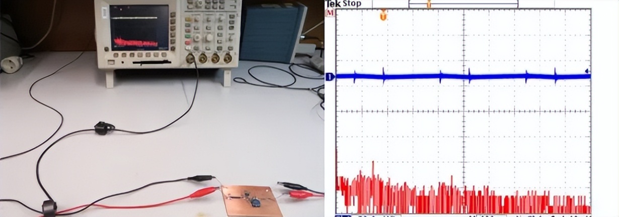
 We first make a routine check for radiation noise by measuring the common-mode current on the input line.
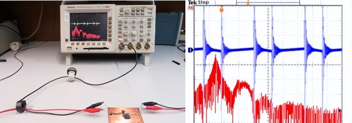 As you can see from the waveform shown on the right side of the image above, the common mode current is surprisingly large and can be seen over a wide entire frequency band.
We can use a ring antenna to search the radiation field above the PCB to find the source of the common mode current. When the loop antenna is moved above the input loop, the oscilloscope shows large radiated noise in the low frequency band up to 200MHz, see the figure below.
We also saw high overshoot and ringing signals on the switching waveform, which actually exceeded the IC's withstand voltage specifications. These conditions indicate that the wrong input capacitor placement can result in high radiation and a large ringing signal.
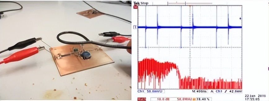 If the same test is performed on a board with a ground layer on the back, we will see that the radiation from this large CIN circuit with a ground layer is much lower than that from a single panel, and the ringing signal caused by the switch is also lower. See the figure below.
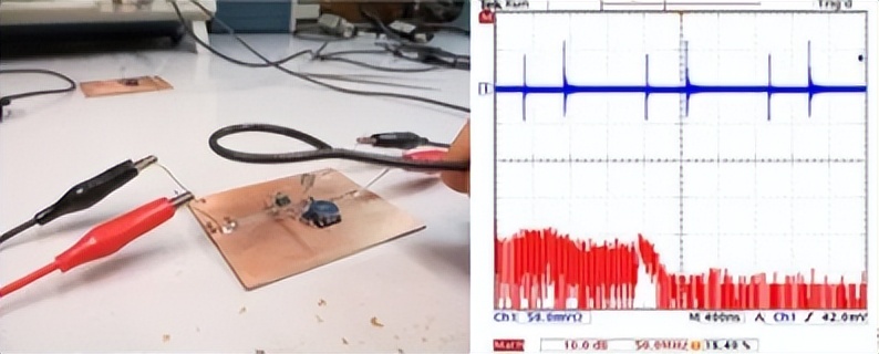 The high frequency magnetic field formed by the current in the large circuit will generate vortex current in the ground layer, and the magnetic field formed by the vortex current is in the opposite direction of the original magnetic field, so that part of the original magnetic field can be offset. The closer the ground layer is to the circuit, the better the effect of cancellation.
Experiment 2: Place CIN close to IC
We continue to use a single-sided PCB and place the CIN close to the IC, thus forming a relatively small CIN loop. See the figure below.
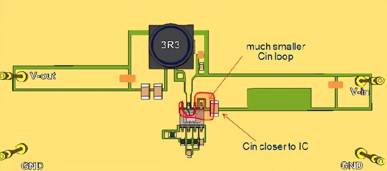 The amplitude of the overshoot and ringing signal during the switching process is reduced by about 50%, the intensity of the radiation is reduced by about 10dB, and the bandwidth is extended to 300MHz.
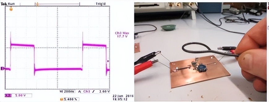 The most important conclusion of the above experiments was to confirm that better placement of CIN can improve the amplitude of overshoot and ringing signals on the switching waveform, and also reduce high frequency radiation.
In RT7297CHZSP, the cooling pad at the bottom of the chip is not connected to the wafer core, so connecting the copper foil and cooling pad together in the PCB layout will not shorten the CIN loop. Its upper bridge MOSFETs and lower bridge MOSFETs are connected to VIN and GND terminals through multiple bond wires, so the shortest loop can be formed through these two terminals.
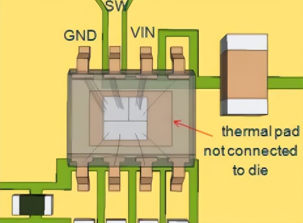 Experiment 3: Add an additional 10nF small capacitor directly between the VIN and GND terminals of the IC
The following figure shows the placement of the capacitor. The CIN loop is now formed by the IC pin, the internal Bonding line, and the 0603 capacitance.
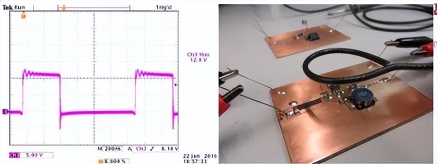
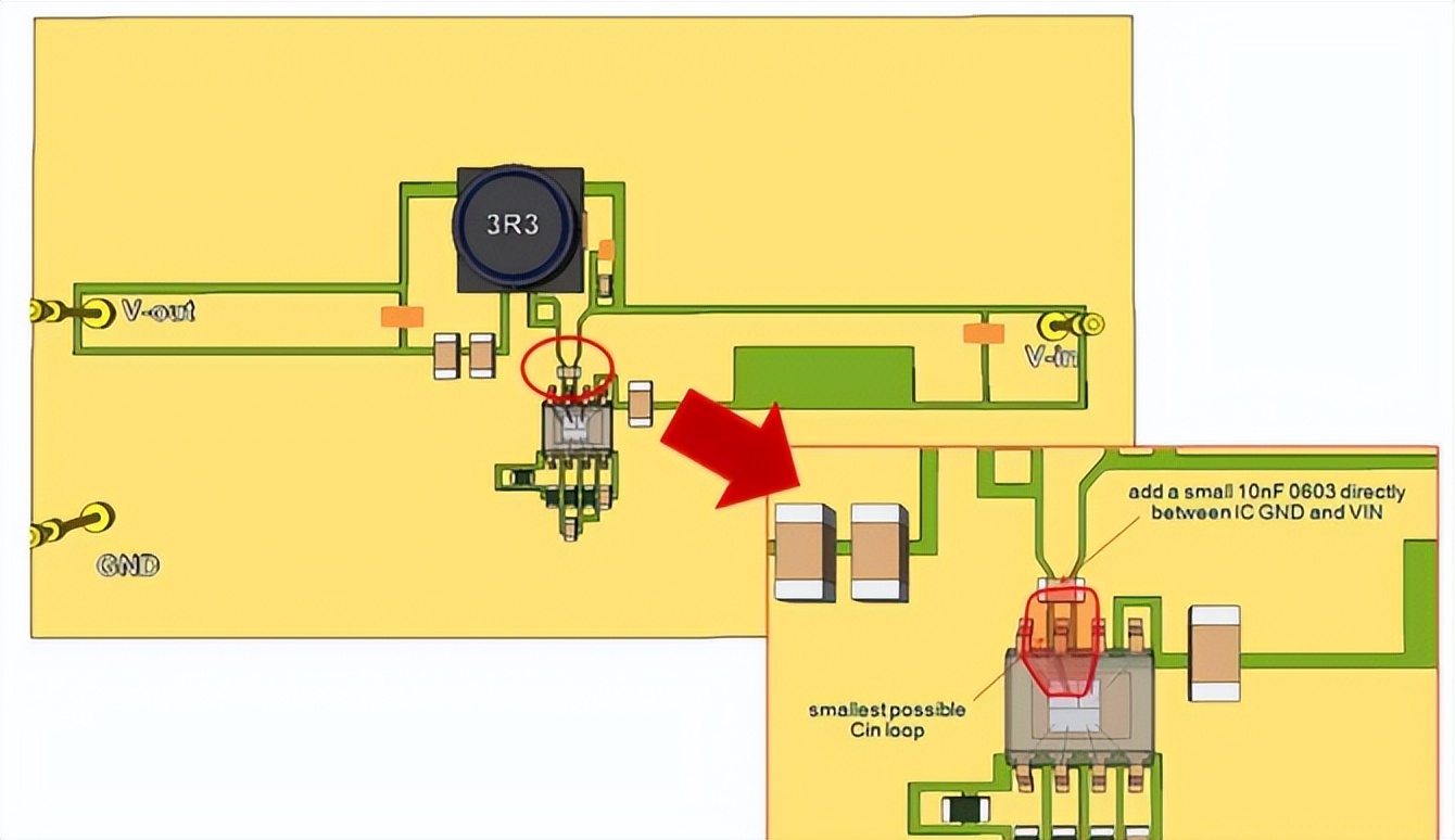 From the experimental results, the overshoot on the switching waveform has actually disappeared, but there is still a low frequency ringing signal.
In order to see the signal, the test antenna also had to move closer to the PCB, which showed that the high-frequency noise had disappeared, but there was a large low-frequency spike at about 25MHz.
This low frequency resonance is often caused by two capacitors in different resonance loops resonating in parallel, this problem often occurs in the process of solving EMI problems, and the loop and resonance need to be located to eliminate. In this case, the resonance occurs on a 10nF capacitor and a 4nH parasitic inductor (about 3mm conductor length), which form a resonant signal of about 25MHz. This resonant loop consists of a 0603 capacitor, IC pin, bond wire and PCB copper foil path, which is approximately 3mm in length.
The solution to this problem is to parallel a 22µF 1206 capacitor with a slightly higher ESR next to a small 10nF capacitor.
The PCB layout design using the optimized CIN placement method is shown in the figure below.
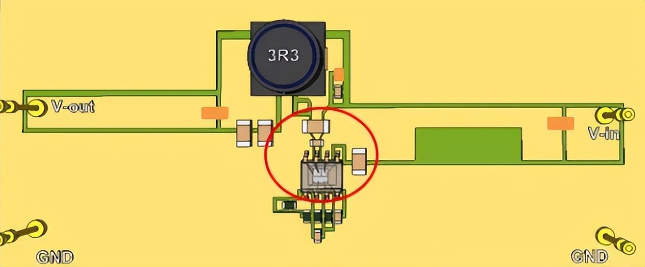 After the above scheme is adopted, the overshoot on the switching waveform on the single panel has completely disappeared, and the radiation noise detected by the ring antenna is also very low, and the waveform obtained after FFT operation is almost at the background noise level.
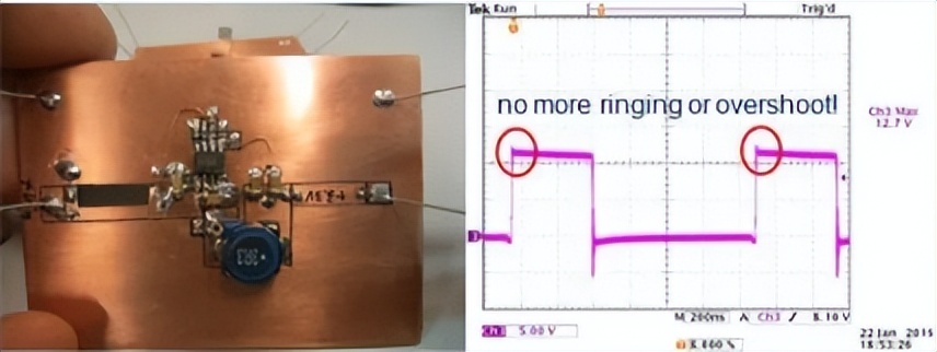 If we use a high-frequency current probe to measure the common-mode current on the input line at this time, we will see that the common-mode noise has decreased a lot. Compared with the results of the first measurement, the difference in some frequencies is more than 30dB, indicating that the radiation level of the entire board is already very low.
 Filter on the power input line
The high frequency current on the power supply input line is composed of differential mode current and common mode current. For common-mode currents, the current loop with a high current change rate dI/dt can be minimized during PCB layout design. The differential mode current has different sources, which can be measured by passing positive and negative lines through the magnetic core of the self-made current probe in different directions as shown in Figure 27.
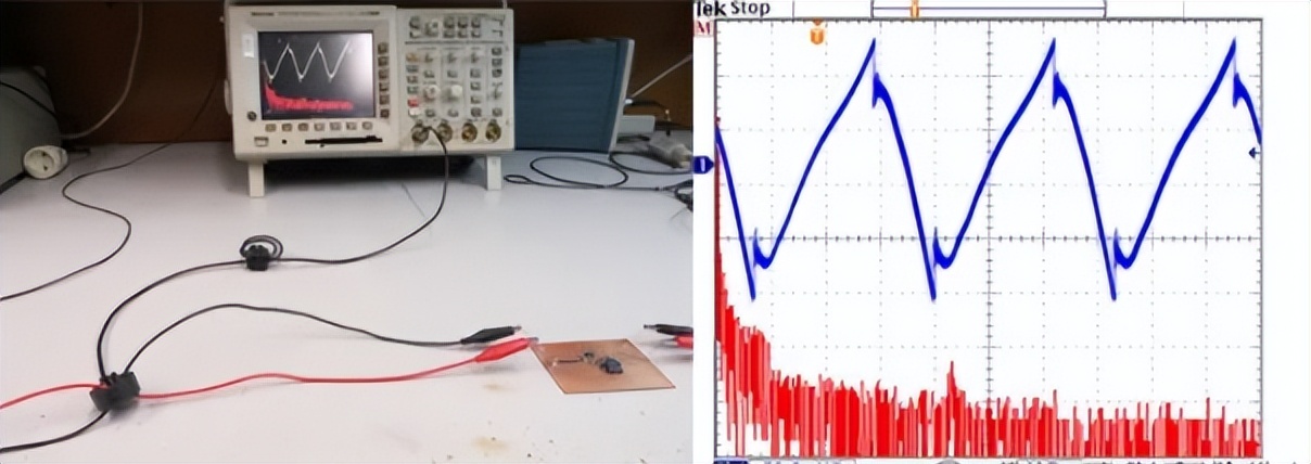 The differential mode current we want to measure is caused by the voltage dip on the input capacitor caused by the pulse input current of the Buck converter as it passes through the input capacitor due to the ESL (if present) formed by its ESR and PCB layout, which finally appears on the power input line as the differential mode current.
The differential mode current can be reduced by increasing the input capacitance, but it is more efficient to add a small LC filter to the input line, as shown on the right side of the figure below.

 As you can see from the above figure, the filter with the addition of magnetic beads + capacitors can remove all high-frequency components except the 800kHz fundamental wave, and the filter with the addition of 1µH inductor + capacitor can eliminate all differential mode noise including the fundamental wave.
Filter on the output line
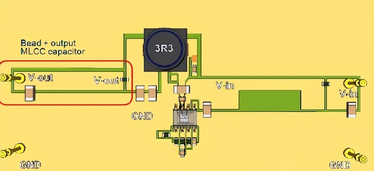
When the differential mode signal at the output is measured, we can see less high-frequency components, because the output current is continuous and the current change rate is not high. However, we can still see low frequency noise up to about 30MHz, which is because the current ripple on the inductor in the converter is passed through the output capacitor to the output as the differential mode current on the output, after all, these capacitors also contain ESR and ESL. Most of the differential mode signal can be filtered out by adding an additional LC filter at the output, which can be composed of magnetic beads and MLCC capacitors, as shown in the following figure.
 One thing that often happens is that the magnetic leakage of some inductors will be coupled to the output circuit, which will also cause the output differential mode current to appear.
The magnetic leakage of the shielded inductor will be relatively low, and the magnetic field signal is not easy to enter the output loop, but the unshielded or semi-shielded inductor is completely different. Once this is the case, the area of the output loop must be minimized so that it cannot easily couple the inductor's magnetic leakage into it.
The ringing signal is reduced by using series resistors in the bootstrap circuit and RC buffer suppression circuit
In this experiment, we use a double-sided PCB, and the input capacitor is placed in the same position as in experiment 2 above, which can introduce more obvious radiation in the input loop.
 For reference, the common-mode current on the input line is first tested without Rboot and RC buffer suppression circuits.
The switching waveform shows a 5V overshoot, and the oscillation frequency of the overshoot signal is 238MHz. The common-mode current on the input line shows obvious high-frequency noise. Refer to the image below.
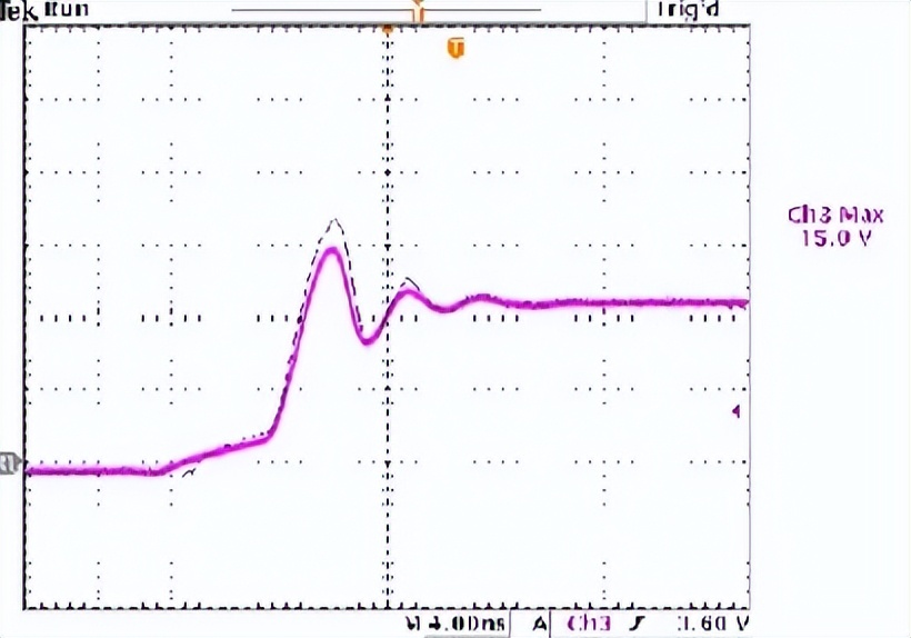
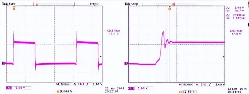 The RT7297C uses a relatively small upbridge MOSFET (110mΩ) and thus has little impact on the bootstrap circuit by connecting small resistors in series. The experiment found that even if Rboot is added to 20Ω, no significant waveform change can be seen. The oscilloscope graph shown in the following figure compares the waveform when the resistance is 0Ω (gray) with the waveform when the series resistance is added to 33Ω, and it can be seen that the overshoot signal amplitude is reduced to 3V. The effect of this change on the common-mode current is also small and hardly noticeable in this simple measurement.
 The value of the RC buffer suppression circuit is determined below
The original frequency of the ringing signal fRING = 238MHz, after adding 220pF capacitor, fRING becomes 114MHz, so CP = 220pF/3 = 73pF.
LP can be calculated by the formula LP = 6.1nH.
 RS can be calculated by a formula. We choose ξ = 0.5, so RS = 9.1Ω, we choose 8.2Ω.
 CS should be 4xCP, so it's 330pF.

Adding RC buffer suppression circuits in high frequency bands can reduce the common-mode current by 5dB.

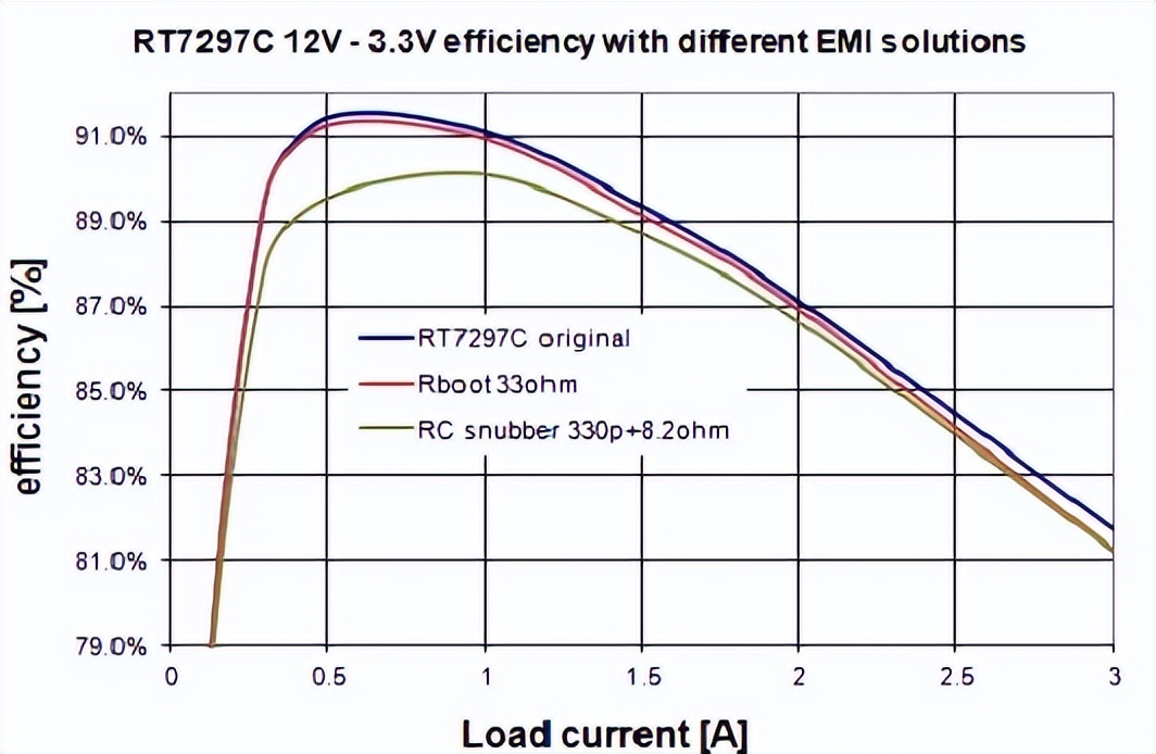
As can be seen from the figure above, the impact of Rboot on efficiency is relatively small, but the impact is increased when the load is heavy.
The effect of the RC smooth suppression circuit on the efficiency will be relatively large, especially in the case of light load and medium load, but the maximum is 1~2%, which is in the acceptable range. It should be noted that when the Buck converter operates at a high frequency and the input voltage is high, the RC smooth suppression circuit will have a great impact on the efficiency.
6. BUCK converter PCB layout design points
The key to Buck converter PCB layout design is to plan the placement of key components at the beginning.
1. In noise-sensitive applications, it is best to choose a small package and a very low inductance wafer flip chip.
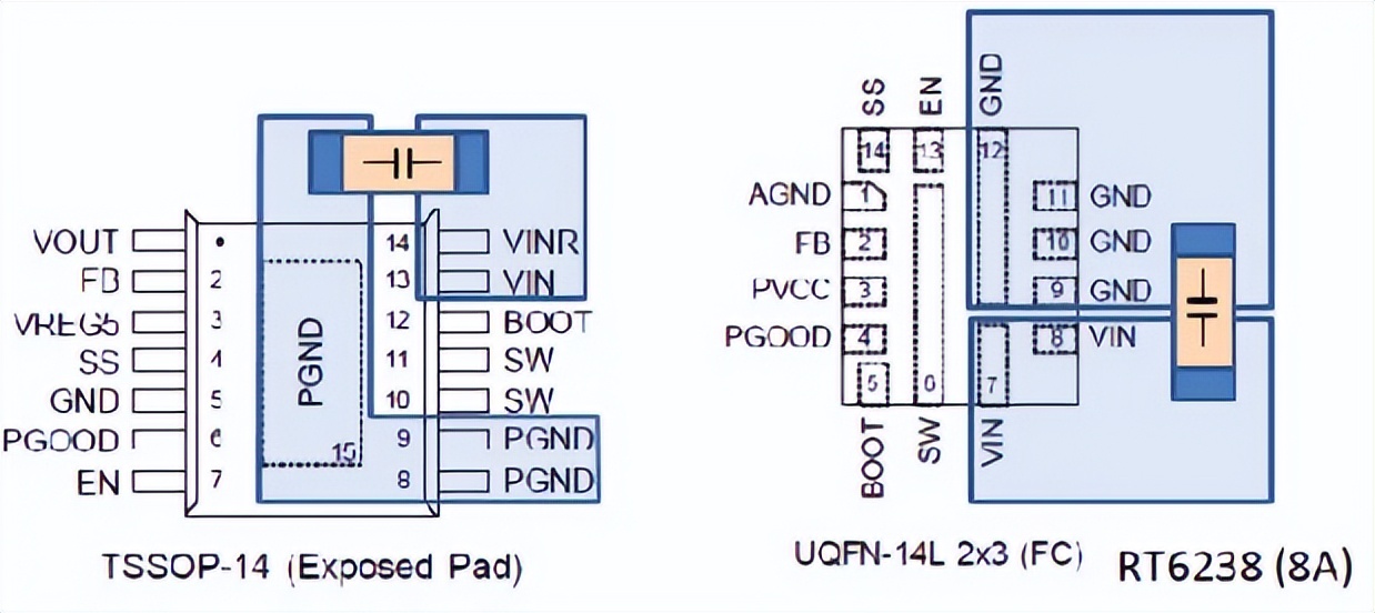 2. Determine the VIN and GND nodes of the switching loop, and place input capacitors of different sizes as close as possible to these nodes, with the smallest capacitor closest to the node. Since this switching loop carries a high current change rate dI/dt, it needs to be as small as possible.
 3. Place the output capacitor in a place that does not overlap with the switching path of the input capacitor to avoid high-frequency noise stringing into the output voltage.
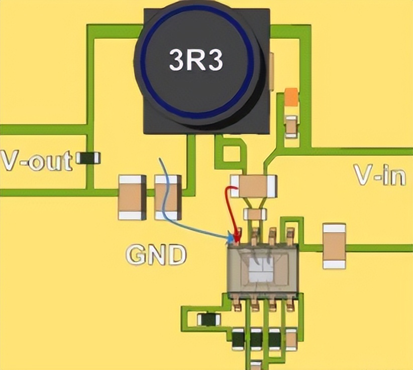 The switching node and BOOT pin contain a high voltage change rate dV/dt, which can cause serious electric field radiation, so the copper foil area should be kept to a minimum, and other sensitive circuits should be avoided.
4. The small signal part of the converter should be separated from the high-power switch switching part, and the ground wire should be located in a clean and noiseless place, and do not introduce the input current signal and the output ripple current into it.
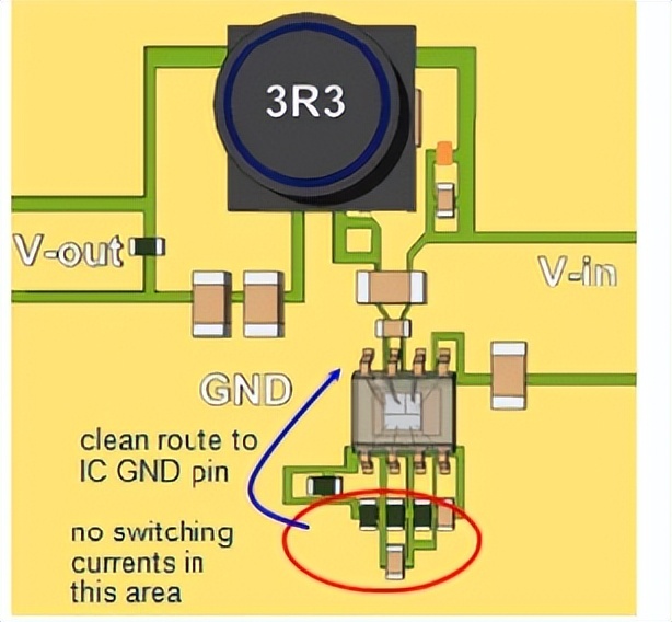 Do not use thermal pads on critical circuits, as they introduce excess inductance characteristics.
5. When using the ground layer, try to maintain the integrity of the ground below the input switching loop. Any cutting of the ground layer in this area will reduce the effectiveness of the ground layer, and even the signal through the hole through the ground layer will increase its impedance.
6. The conduction hole can be used to connect the decoupling capacitor and IC to the ground ground layer, which can minimize the loop. However, it is important to keep in mind that the inductance of the through-hole is about 0.1 to 0.5nH, which will vary depending on the thickness and length of the through-hole, which can increase the total circuit inductance. For connections with low impedance, it is advisable to use multiple through-holes.
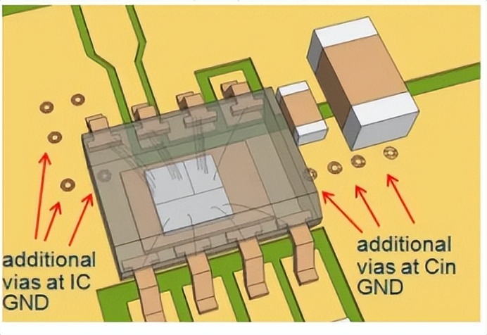 In the above example, additional through-holes to the ground layer do not help reduce the length of the CIN loop. But in another example, because the top layer of the path is very long, through the hole to reduce the loop area is very effective.
7. It should be noted that taking the ground layer as the path of current return will introduce a large amount of noise into the ground layer, so the local ground layer can be independently separated and then connected to the main ground through a point with low noise.
8. When the local wire layer is very close to the radiation circuit, its shielding effect on the circuit will be effectively strengthened. Therefore, when designing a multi-layer PCB, the complete ground line layer can be placed on the second layer, so that it is directly located under the top layer that carries a large current.
9. Unshielded inductors will generate a large amount of magnetic leakage, which will enter other loops and filter elements. Semi-shielded or fully shielded inductors should be used in noise-sensitive applications, and sensitive circuits and loops should be kept away from the inductor.
7. Simple EMI problem detection tools that you can make yourself
Measuring EMC problems usually means you have to take your prototype to the EMC lab for testing. There are usually 3m echo free rooms with special measurement equipment using antennas and receivers. The measurement data can show the final result of the entire system. But in such places it is not always easy to find the root cause of a particular radiation problem.
In fact, it is possible to perform some basic EMI tests on the product prototype in the laboratory environment, and also perform individual modules of the system. Such tests are usually in near-field environments (measuring distances < 0.16λ), so a small loop antenna is needed to measure the high-frequency magnetic field when testing the radiation status of the current loop. You can use a 50Ω coaxial cable to make your own small ring antenna with electrical shielding, this does not seem to be a difficult thing, you can refer to the diagram below.
 This loop antenna can be connected to a spectrum analyzer, and when you move it over the PCB, you can see where there will be a strong high-frequency magnetic field. You can also connect it to an oscilloscope (using 50Ω terminals) and the oscilloscope will display the switching noise level for the corresponding area. Keep the relative position and distance between the antenna ring and the board unchanged, make certain changes to the circuit, the circuit on the PCB, and you can tell whether the noise level is increasing or decreasing.
Since the radiation from the power lines has a big impact on EMI levels, you can also measure the high frequency current on these lines. Not all current probes have enough bandwidth to highlight EMI problems, which can be solved by passing a few turns of coil through an EMI core to form a high-frequency current transformer. The method is similar to that of a ring antenna, but the ring coil needs to be passed through the core three times. See the figure below.
 The high frequency current can now be measured by running the cable through the core, and the output of the current transformer can be plugged into a spectrograph or oscilloscope (using a 50Ω port).
In order to separate the test tool from the test object, it is best to add a common mode coil to the cable, which can be achieved by running the cable leading into the analysis device through a buttoned EMI core several times.
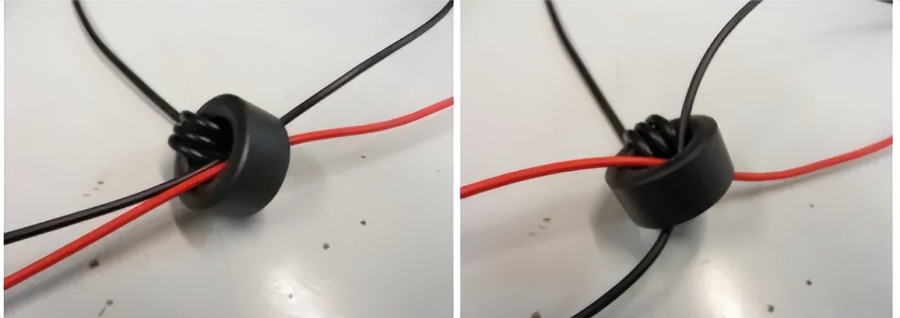 The common mode current can be measured by passing the positive and negative lines of the power cord through the iron core in the same direction, and the differential mode current can be measured by reversing the direction of one of the lines. See the picture above.
Another handheld tool is the current detector, a miniaturized current transformer with an open core, as shown below. This tool can be used to measure high frequency currents on copper foil paths or component pins.
 This tool will be difficult to make, you can use a ferrite magnetic bead with two holes after grinding to get an open core, plus 4 to 5 turns of coil, and then connect it to the coaxial cable. It is best to place the core in a shield with an opening. When using this tool, you should be aware that it will also pick up some electric field signals. To tell if your measurement is coming from a magnetic or electric field, you can turn the tool 90 degrees above the path. If the measurement comes from a magnetic field, the result will be 0. If the signal comes from an electric field, the result will not change.
 The current detector lets you know how the changing high frequency current flows on the plate and components, and can even show how the current flows on the copper foil: you will find that the high frequency current always passes the shortest path on the copper foil. In fact, even eddies in the ground layer can be measured.
8. Summary
Solving EMI problems can be complicated, especially when dealing with complete systems and not knowing where the radiation is coming from. With a basic knowledge of high frequency signals and current loops in switch-over converters, coupled with an understanding of how components and PCB layouts behave at high frequencies, combined with the use of some simple homemade tools, it is possible to easily solve EMI problems by identifying radiation sources and low-cost solutions to reduce radiation.
The main radiation source in Buck converter is the input switching loop of the converter, which is the focus of our consideration. Switching converters in different packages have the potential to play a very important role in obtaining the optimal component layout for the solution with the lowest EMI radiation.
Reducing the switching speed of the converter can help reduce EMI, but this is usually not the optimal choice. Shielding through ground layers is a very effective practice, they should be as large and complete as possible, but also as close as possible to the radiating loop. Filtering the input and output lines can be very effective in reducing the level of conducted radiation.


